I was recently tinkering with an old radio, a classic crystal set, and it struck me how utterly dependent modern electronics are on tiny, invisible components: **semiconductors**. These fundamental building blocks, from the silicon chip in your smartphone to the processors in supercomputers, are the bedrock of our digital age. But as I traced the simple wires and marveled at the rectifying crystal, a peculiar thought sparked in my mind: *Could ancient civilizations, particularly the technologically astute Romans, have stumbled upon or even understood rudimentary forms of semiconductor technology?*
It sounds like a far-fetched idea, doesn't it? We typically associate semiconductors with 20th-century physics and advanced material science. Yet, the Romans were masters of metallurgy, chemistry, and engineering. They built structures that have stood for millennia, perfected concrete that could self-heal, and crafted intricate glasswork that still baffles modern scientists. Considering their deep empirical knowledge of materials, it’s not entirely unreasonable to ask if they might have, perhaps inadvertently, created materials or structures exhibiting semiconductor-like properties.
### The Unseen World of Roman Innovation
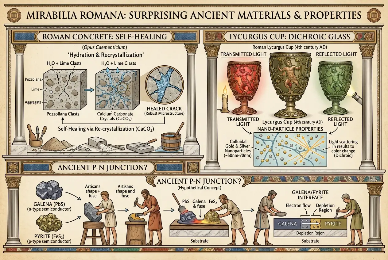
The Roman Empire was not just about legions and aqueducts; it was a crucible of practical innovation. Their understanding of materials was profound, even if their theoretical framework differed from ours. For instance, their mastery of alloys, pigments, and glass production reached levels arguably unmatched until the Industrial Revolution. We see this in their stunning artistry, like the **Lycurgus Cup**, a 4th-century Roman cage cup made of dichroic glass that changes color depending on whether light passes through it or reflects off it. This effect, as we now understand, is due to nanoparticles of gold and silver embedded in the glass – a feat of ancient nanotechnology. For more on this fascinating artifact, you can delve into its secrets in our previous blog: [Lycurgus Cup: Did Romans Use Quantum Tech?](/blogs/lycurgus-cup-did-romans-use-quantum-tech-3796).
Their vast knowledge wasn't confined to art. Roman engineers built impressive infrastructure, and their understanding of various ores and minerals was critical. They processed lead, copper, iron, gold, and silver on an industrial scale. This constant experimentation with heating, smelting, and combining different elements could have led to unforeseen material properties.
### What Exactly Is a Semiconductor?
Before we dive deeper into potential Roman "diodes," let's briefly define what a semiconductor is. At its core, a **semiconductor** is a material with electrical conductivity between that of a conductor (like copper) and an insulator (like glass). Crucially, their conductivity can be controlled. This property arises from their atomic structure and how electrons are shared.
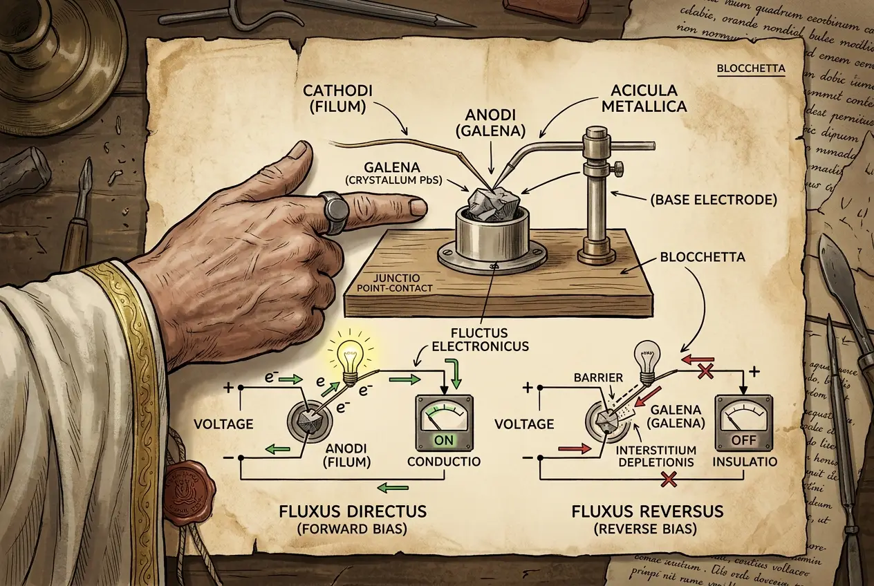
The simplest form of a semiconductor device is a **diode**, which acts like a one-way valve for electricity. It allows current to flow easily in one direction but strongly resists it in the opposite direction. This rectifying behavior is fundamental to converting alternating current (AC) to direct current (DC), detecting radio waves, and forming the basis of all digital logic. Modern diodes are typically made from silicon or germanium, precisely "doped" with impurities to create P-type (positive charge carriers) and N-type (negative charge carriers) regions that form a junction. You can read more about semiconductors on [Wikipedia](https://en.wikipedia.org/wiki/Semiconductor).
### Candidates for Ancient Semiconductors: Natural Minerals
While Romans certainly didn't have the quantum mechanics to dope silicon, nature provides several minerals that are natural semiconductors. These minerals were readily available and often used by ancient civilizations for various purposes.
1. **Galena (Lead Sulfide):** This shiny, metallic-looking mineral was a common lead ore and was known to the Romans. Interestingly, galena is one of the earliest known natural semiconductors. In the early 20th century, before vacuum tubes, **galena crystals were used in "crystal radio" sets** as a point-contact rectifier, effectively acting as a diode to detect radio waves. It's a surprisingly effective natural semiconductor. The Romans certainly encountered and processed galena. While they might not have understood its electrical properties, could certain preparations or uses have leveraged them? More on galena's properties can be found on [Wikipedia](https://en.wikipedia.org/wiki/Galena).
2. **Pyrite (Iron Sulfide):** Often mistaken for gold, pyrite was also known and sometimes used by ancient cultures. It, too, exhibits semiconducting properties. Its crystalline structure and composition make it a less efficient rectifier than galena, but still a candidate for rudimentary semiconductor behavior.
3. **Copper Oxides:** The Romans extensively mined and processed copper. When copper oxidizes, it can form various compounds, including **copper(I) oxide (Cu₂O)**, which is a p-type semiconductor. This compound can naturally form layers on copper surfaces or within copper alloys when exposed to specific heat and atmospheric conditions. Imagine a copper artifact, perhaps a tool or a decorative element, that underwent a particular firing or weathering process. Could layers of copper oxide have formed that, when accidentally contacted with another dissimilar material, created a rectifying junction? Early industrial rectifiers actually used copper oxide. Learn more about copper(I) oxide on [Wikipedia](https://en.wikipedia.org/wiki/Copper(I)_oxide).
### The Hypothesis: Accidental Diodes?
The idea isn't that Romans intentionally built silicon chips. It's more nuanced:
* **Empirical Discovery:** Through countless trials with various ores, heating techniques, and mixing elements, artisans might have occasionally produced materials or interfaces that exhibited unusual electrical behavior. Perhaps a specific type of slag, a byproduct of smelting, or a particular patina on a metal surface, might have inadvertently possessed these properties.
* **Unintentional Junctions:** A diode requires a junction between two different types of semiconducting material (P-type and N-type). Could natural processes, or ancient manufacturing techniques, have created such interfaces? For example, if a piece of galena (a natural semiconductor) was used in proximity to another material that served as a "point contact" or formed an oxide layer with different electrical properties, it could have formed a crude rectifier.
* **Lost Knowledge of "Anomalous" Materials:** Ancient texts often speak of materials with strange or wondrous properties. Could some of these descriptions refer to substances that, in retrospect, displayed electrical anomalies that we would now categorize as semiconductor behavior? Without the theoretical framework of electricity, these observations might have been attributed to magic, divine intervention, or simply curious quirks.
### How Might They Have Been Used (Hypothetically)?
If some Roman artifacts or materials did indeed possess rudimentary semiconductor properties, how might they have been used?
* **Primitive Sensors:** A material sensitive to light (a photodiode effect) or temperature changes could have been incorporated into devices that indicated environmental shifts.
* **Simple Rectifiers:** Imagine a scenario where a weak, naturally occurring electrical current (perhaps from early "batteries" like the one found in Baghdad, see our blog: [Baghdad Battery: Did Ancients Spark Our Electric Age?](/blogs/baghdad-battery-did-ancients-spark-our-electric-age-7832)) was present. A rudimentary diode could have converted this pulsating current into a more stable direct current, even if the scale was minuscule.
* **Radio Wave Detection (Very Speculative):** If point-contact rectifiers similar to crystal radio detectors existed, it raises the thrilling, albeit highly speculative, question of whether they could have detected any natural electromagnetic phenomena.
One of the greatest achievements of Roman metallurgy was **Damascus steel**, renowned for its incredible strength and sharpness, attributed to its unique microstructure, which modern analysis has shown involved carbon nanotubes and nanowires. This suggests a level of material control and an empirical understanding that pushed the boundaries of what we consider "ancient." You can explore more about this incredible material here: [Damascus Steel: Was Ancient Tech Stronger Than Modern?](/blogs/damascus-steel-was-ancient-tech-stronger-than-modern-7964). If they could manipulate materials to create such complex structures, could they have also accidentally or purposefully created semiconductor junctions?
### The Elusive Evidence
The challenge, of course, lies in finding definitive archaeological evidence. Unlike the Antikythera Mechanism, a complex mechanical calculator that clearly points to advanced Greek computational abilities, a "Roman diode" would be much harder to identify. It might be a small inclusion in an alloy, a specific layered patina, or an interface between two materials that only reveals its electrical properties under modern scrutiny. It would require scientists to re-examine ancient artifacts not just for their artistic or historical value, but for their hidden electronic characteristics.
Recent advancements in material science and archaeological analysis, using techniques like scanning electron microscopy and spectroscopy, are allowing us to look at ancient artifacts with unprecedented detail. Who knows what secrets the atomic structure of a Roman coin or a piece of glass might still hold? The very possibility encourages us to view the past not as a static, primitive era, but as a dynamic period of intense experimentation and often surprising technological achievement.
The pursuit of such anomalies isn't about rewriting history with outlandish claims, but about opening our minds to the sheer ingenuity and empirical depth of ancient civilizations. They understood their world through observation and craftsmanship in ways we are only beginning to fully appreciate.
Could a Roman artisan, unknowingly, have crafted a material that functioned as a rudimentary semiconductor? While direct proof remains elusive, the depth of Roman material science, coupled with the natural availability of semiconducting minerals, suggests that the possibility, however remote, is a fascinating one to ponder. It pushes us to question our assumptions about technological progression and to look for the echoes of advanced understanding in the most unexpected places. The next time you hold a piece of ancient Roman pottery or admire a metal artifact, consider the unseen secrets it might still hold.
Frequently Asked Questions
Romans commonly encountered minerals like galena (lead sulfide) and pyrite (iron sulfide), which are natural semiconductors. Copper(I) oxide, a p-type semiconductor, could also form naturally on copper artifacts through oxidation processes.
Through extensive experimentation with ores, heating techniques, and combining elements, Roman artisans might have unintentionally produced materials or interfaces that exhibited rectifying electrical behavior, such as a layered patina or specific slag byproducts from smelting.
Currently, there is no direct archaeological evidence of intentionally designed Roman semiconductor devices like modern diodes. The hypothesis focuses on the possibility of accidental creation of materials or junctions with semiconductor-like properties due to their advanced material science.
The Lycurgus Cup, a Roman artifact, demonstrates their mastery of nanotechnology through its dichroic glass embedded with gold and silver nanoparticles. This shows a sophisticated empirical understanding of materials, suggesting they could have manipulated other substances in ways we are only beginning to understand.
Modern scientific techniques like scanning electron microscopy, X-ray diffraction, and spectroscopy can be used to re-examine ancient Roman artifacts at a microscopic level, looking for unusual material interfaces, crystalline structures, or compositions that might indicate rudimentary semiconducting properties.
Verified Expert
Alex Rivers
A professional researcher since age twelve, I delve into mysteries and ignite curiosity by presenting an array of compelling possibilities. I will heighten your curiosity, but by the end, you will possess profound knowledge.
Leave a Reply
Comments (0)
No approved comments yet. Be the first to share your thoughts!
 Join Us


 Alex Rivers


Leave a Reply
Comments (0)